- 半導體首頁
-
應用Automotive
Body Electronics
xEV
In-Vehicle Infotainment
Advanced Driver-Assistance Systems (ADAS)
Chassis
IndustrialInfrastructure
BEMS/HEMS
Factory Automation
Commercial Equipment
Consumer/PersonalIoT Equipment
Healthcare
Wearable Device
Mobile
Computer Peripherals
-
產品車用元件
Discrete Semiconductor
Diodes
電晶體
通用邏輯IC
Analog Devices
Digital Devices
Wireless Devices
※
: Products list (parametric search)
功率半導體※
: Products list (parametric search)
隔離器/固態繼電器Photocouplers
Digital Isolators
※
: Products list (parametric search)
MOSFETsIGBTs/IEGTs雙極性電晶體※
: Products list (parametric search)
Diodes※
: Products list (parametric search)
微控制器馬達驅動 ICs智能功率 ICs※
: Products list (parametric search)
電源管理 ICs線性 ICs※
: Products list (parametric search)
通用邏輯 ICs線性影像感測器其他產品其他產品
※
: Products list (parametric search)
-
開發/設計支援
開發 / 設計支援
-
技術知識
- 購買管道
- 型號 & 關鍵字搜尋
- 交叉搜尋
- 參數搜尋
- 線上庫存查詢跟購買
This webpage doesn't work with Internet Explorer. Please use the latest version of Google Chrome, Microsoft Edge, Mozilla Firefox or Safari.
型號需要超過三個文字以上 Search for multiple part numbers fromhere.
The information presented in this cross reference is based on TOSHIBA's selection criteria and should be treated as a suggestion only. Please carefully review the latest versions of all relevant information on the TOSHIBA products, including without limitation data sheets and validate all operating parameters of the TOSHIBA products to ensure that the suggested TOSHIBA products are truly compatible with your design and application.Please note that this cross reference is based on TOSHIBA's estimate of compatibility with other manufacturers' products, based on other manufacturers' published data, at the time the data was collected.TOSHIBA is not responsible for any incorrect or incomplete information. Information is subject to change at any time without notice.
型號需要超過三個文字以上
What is the gate-driver that facilitates the overcurrent protection design of inverter applications?
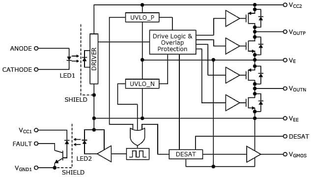
The pre-driver TLP5231 is suitable for industrial inverters and photovoltaic power conditioning systems as a medium to high current IGBT/MOSFET driver, with a built-in overcurrent detecting function and a soft turn-off function. The TLP5231 also provides over-current protection with DESAT short-circuit detection that monitors the collector voltage of an IGBT or the drain voltage of a MOSFET. This function detects overcurrent and softly turns off the IGBT/MOSFET gate-voltage. This soft turn-off feature prevents fatal overcurrent caused by short-circuiting through the power devices for both high-side and low-side.
In addition, the conventional IGBT/MOSFET drive photocoupler only stops operation when UVLO [Note 1] is working, but the TLP5231 outputs a fault signal to the primary side when UVLO is working, supporting the design as a pre-driver more than a conventional IGBT/MOSFET.
Since the TLP5231 drives medium to high current MOSFET and IGBT gates via the p-channel and n-channel complementary buffer MOSFETs, the current flows to charge or discharge the buffer MOSFET, resulting in low power consumption. It is possible to create the required gate current for various IGBTs / MOSFETs simply by changing the external complementary buffer MOSFET size. By using a platform that combines TLP5231 with buffer MOSFETs and IGBT/MOSFET it is possible to cover a wide line-up system power sizes and contribute to reducing design workload.
[Note 1] UVLO: Under voltage lockout
Application
- Industrial inverters and Uninterruptible Power Supplies (UPS)
- Photovoltaic power conditioning system
Features
- Reduce the workload of dead-time design
2. Improve the design flexibility for the soft turn-off
3. Fault signal auto-reset
1. Reduce the workload of dead-time design
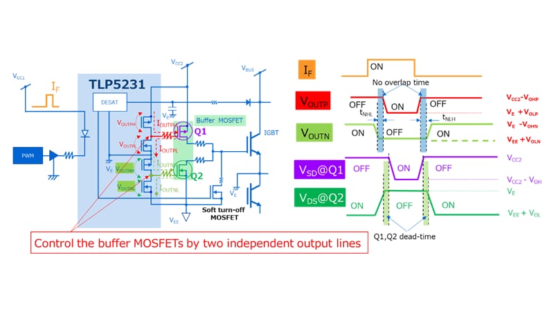
TLP5231 has two output lines to control buffer MOSFET Q1 / Q2 and provides a time difference (non-overlap time) between the ON / OFF signals of Q1 / Q2 to ensure dead-time when turning off both Q1 and Q2. This dual-output eliminates the need for dead-time design, which was difficult due to the buffer configuration with bipolar transistors, and prevents switching loss due to simultaneous ON-state generation.
2. Improve the design flexibility of soft turn-off
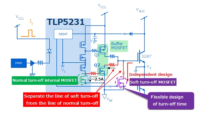
TLP5231 requires an additional MOSFET for soft turn-off in the event of an anomaly. Since this soft turn-off MOSFET doesn’t share wires (lines) with buffer MOSFET Q2, flexible design is possible without worrying about trade-off with normal OFF-operation.
3. Fault signal auto-reset
The gate circuit of a power device controlling high voltages is very noisy, and DESAT monitoring is often falsely detected. To separate overcurrent detection due to anomaly from false detection of noise, as an example, there is a method to stop the system when fault signals are detected multiple times. In this case, if recovery from an abnormal stop is auto-reset type, the MCU doesn’t need to issue a reset signal for each fault signal. And the operation is simplified because the system can stop the machine after counting the specific number of fault signals. As a result, the designer can improve the stability of system operation.
Application Information
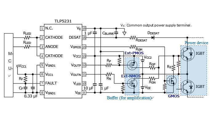
Ext-PMOS: p-channel MOSFET (for current-buffer)
Ext-NMOS: n-channel MOSFET (for current-buffer)
GMOS: n-channel MOSFET (for soft turn-off control)
NOTE: This application circuit example is for reference only, and the designer should thoroughly evaluate it for mass production. In addition, it does not permit the use of Industrial Property Rights.
Internal Circuit
Main specifications of the new product
(@Ta =-40 to 110 °C unless otherwise specified)
Product Number |
||
|---|---|---|
Absolute maximum rating |
Peak high level output current IOPH (A) |
-2.5 |
Peak low level output current IOPL (A) |
+2.5 |
|
Electrical Characteristics |
VOUTP high level output current IOUTPH max (A) |
-1.0 |
VOUTP low level output current IOUTPL min (A) |
1.0 |
|
VOUTN high level output current IOUTNH max (A) |
-1.0 |
|
VOUTN low level output current IOUTNL min (A) |
1.0 |
|
High level supply current (VCC2) ICC2H max (mA) |
10.2 |
|
Low level supply current (VCC2) ICC2L max (mA) |
10.2 |
|
High level supply current (VEE) IEEH min (mA) |
-9.2 |
|
Low level supply current (VEE) IEEL min (mA) |
-9.2 |
|
Threshold input current (H/L) IFHL max (mA) |
3.5 |
|
Recommended operating conditions |
Total output supply voltage (VCC2-VEE) (V) |
21.5 to 30 |
Negative output supply voltage (VE-VEE) (V) |
-15 to -6.5 |
|
Positive output supply voltage (VCC2-VE) (V) |
15 to 23.5 |
|
Switching characteristic |
Propagation delay time (L/H) tpLH (ns) |
100 to 300 |
Propagation delay time (H/L) tpHL (ns) |
100 to 300 |
|
Propagation delay skew tpsk (ns) |
-200 to 200 |
|
High-level common-mode transient tolerance CMH min (kV/μs) |
±25 |
|
Low-level common-mode transient tolerance CML min (kV/μs) |
±25 |
|
Protective function |
Feedback (FAULT): Operates when a VCE(sat) is detected or a UVLO is detected (open collector output). |
|
Isolation Characteristics (@Ta=25 °C) |
Isolation voltage BVS min (Vrms) |
5000 |
Structural parameter |
Clearance distance min (mm) |
8.0 |
Creepage distance min (mm) |
8.0 |
|
Insulation thickness min (mm) |
0.4 |
|
[Note] VE standard
※ Company name · Product name · Service name may be used by other companies as trademarks.

