- 半導體首頁
-
應用Automotive
Body Electronics
xEV
In-Vehicle Infotainment
Advanced Driver-Assistance Systems (ADAS)
Chassis
IndustrialInfrastructure
BEMS/HEMS
Factory Automation
Commercial Equipment
Consumer/PersonalIoT Equipment
Healthcare
Wearable Device
Mobile
Computer Peripherals
-
產品車用元件
Discrete Semiconductor
Diodes
電晶體
通用邏輯IC
Analog Devices
Digital Devices
Wireless Devices
※
: Products list (parametric search)
功率半導體※
: Products list (parametric search)
隔離器/固態繼電器Photocouplers
Digital Isolators
※
: Products list (parametric search)
MOSFETsIGBTs/IEGTs雙極性電晶體※
: Products list (parametric search)
Diodes※
: Products list (parametric search)
微控制器馬達驅動 ICs智能功率 ICs※
: Products list (parametric search)
電源管理 ICs線性 ICs※
: Products list (parametric search)
通用邏輯 ICs線性影像感測器其他產品其他產品
※
: Products list (parametric search)
-
開發/設計支援
開發 / 設計支援
-
技術知識
- 購買管道
- 型號 & 關鍵字搜尋
- 交叉搜尋
- 參數搜尋
- 線上庫存查詢跟購買
This webpage doesn't work with Internet Explorer. Please use the latest version of Google Chrome, Microsoft Edge, Mozilla Firefox or Safari.
型號需要超過三個文字以上 Search for multiple part numbers fromhere.
The information presented in this cross reference is based on TOSHIBA's selection criteria and should be treated as a suggestion only. Please carefully review the latest versions of all relevant information on the TOSHIBA products, including without limitation data sheets and validate all operating parameters of the TOSHIBA products to ensure that the suggested TOSHIBA products are truly compatible with your design and application.Please note that this cross reference is based on TOSHIBA's estimate of compatibility with other manufacturers' products, based on other manufacturers' published data, at the time the data was collected.TOSHIBA is not responsible for any incorrect or incomplete information. Information is subject to change at any time without notice.
型號需要超過三個文字以上
3rd generation SiC Schottky barrier diode
The 3rd generation Silicon Carbide (SiC) Schottky barrier diode (SBD) has a lineup of seven products parts of TO-220-2L package and 5 products of DFN8×8 package. It adopts the new schottky metal [Note 1], and it is equipped with 3rd generation SiC SBD chip, which optimized junction barrier schottky (JBS) [Note 2] structure of 2nd generation. As a result, we have achieved industry-leading lowest forward voltage 1.2 V (Typ.) [Note 3], which is 17 % lower than that of the 2nd generation 1.45 V (Typ.). Our 3rd generation SiC SBD contribute to lower power consumption and higher output of various equipment, which is used for switching power supply application mainly, by the following features.
Features of the 3rd generation SiC SBD
1. VF × QC [Note 5] trade-off improvement
We have improved the Forward voltage (VF) and the Total capacitive charge (QC) trade-off by adopting the new Schottky metal.
Below the comparison evaluation results using representative samples of 650V / 10A / TO-220-2L rating products of our 3rd and 2nd generations and other competitors products [Note 3] and 1200V / 20A / TO-247-2L rating produts of our 3rd and other competitors products [Note 4] .
![V<sub>F</sub> × Q<sub>C</sub> <sup>[note5]</sup> trade-off improvement](/content/dam/toshiba-ss-v3/master/en/semiconductor/product/diodes/articles/3rd-generation-sic-schottky-barrier-diode_features_1_en.png)
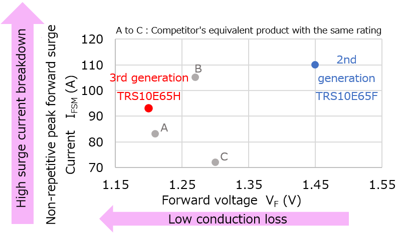
We have achieved higher Non-repetitive peak forward surge current (IFSM) by improving the conventional JBS structure.

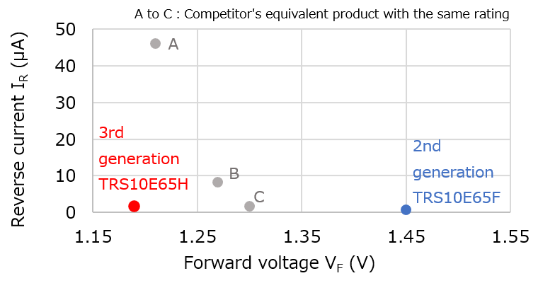
3. Low Reverse current (Leakage current)
We could get lower Reverse current (IR) by adopting JBS structure even through lower Forward voltage.

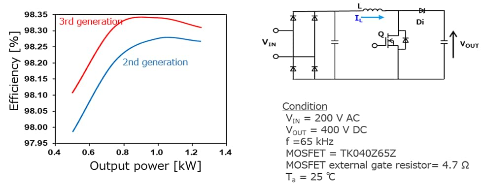
Efficiency improvement of power supply
On our Boost PFC test circuit, our 3rd generation SiC SBD achieved approximately 0.1 % efficiency improvement against 2nd generation at the 800W output condition.

(Toshiba internal comparison, as of November 2021)
[Note 1] In Schottky barrier diodes, it is the metal that is joined to the semiconductor.
[Note 2] JBS: It is a structure which the p region is embedded in the n-regions of the semiconductor surface. When the reverse bias voltage increases, the depletion region extends between the p and n- regions thereby reducing laekage current.
[Note 3] As of June 2023.
[Note 4] As of September 2024.
[Note 5] VF × QC: Forward voltage × total capacitance charge, which is an index of the loss performance of SiC SBD. When you compare with the same current rating products, the smaller VF × QC achieves lower loss.
SiC schottky barrier diodes
Related information
See the following pages for various applications.
See the following pages for Application Notes.
FAQ
See the following page for frequently asked questions.
Queries about purchasing, sampling and IC reliability
線上庫存查詢跟購買
型號需要超過三個文字以上
Through this website you are able to proceed to the website of our distributors ("Third Party Website") which is not under the control of Toshiba Corporation and its subsidiaries and affiliates (collectively "Toshiba"). The Third Party Website is made available to you as a convenience only and you agree to use the Third Party Website at your own risk. The link of the Third Party Website does not necessarily imply a recommendation or an endorsement by Toshiba of the Third Party Website. Please be aware that Toshiba is not responsible for any transaction done through the Third Party Website, and such transactions shall be subject to terms and conditions which may be provided in the Third Party Website.

