
- 半導體首頁
-
應用Automotive
Body Electronics
xEV
In-Vehicle Infotainment
Advanced Driver-Assistance Systems (ADAS)
Chassis
IndustrialInfrastructure
BEMS/HEMS
Factory Automation
Commercial Equipment
Consumer/PersonalIoT Equipment
Healthcare
Wearable Device
Mobile
Computer Peripherals
-
產品車用元件
Discrete Semiconductor
Diodes
電晶體
通用邏輯IC
Analog Devices
Digital Devices
Wireless Devices
※
 : Products list (parametric search)功率半導體
※
: Products list (parametric search)隔離器/固態繼電器Photocouplers
Digital Isolators
※
: Products list (parametric search)MOSFETsIGBTs/IEGTs雙極性電晶體※
: Products list (parametric search)Diodes※
: Products list (parametric search)微控制器馬達驅動 ICs智能功率 ICs※
: Products list (parametric search)電源管理 ICs線性 ICs※
: Products list (parametric search)通用邏輯 ICs線性影像感測器其他產品其他產品
※
: Products list (parametric search) -
開發/設計支援
開發 / 設計支援
-
技術知識
- 購買管道


- 型號 & 關鍵字搜尋
- 交叉搜尋
- 參數搜尋
- 線上庫存查詢跟購買
This webpage doesn't work with Internet Explorer. Please use the latest version of Google Chrome, Microsoft Edge, Mozilla Firefox or Safari.
型號需要超過三個文字以上 Search for multiple part numbers fromhere.
The information presented in this cross reference is based on TOSHIBA's selection criteria and should be treated as a suggestion only. Please carefully review the latest versions of all relevant information on the TOSHIBA products, including without limitation data sheets and validate all operating parameters of the TOSHIBA products to ensure that the suggested TOSHIBA products are truly compatible with your design and application.Please note that this cross reference is based on TOSHIBA's estimate of compatibility with other manufacturers' products, based on other manufacturers' published data, at the time the data was collected.TOSHIBA is not responsible for any incorrect or incomplete information. Information is subject to change at any time without notice.
型號需要超過三個文字以上
TLCS-900/H1 Series Development System
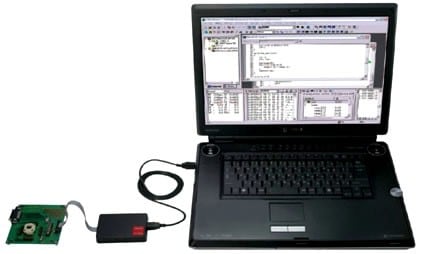
The RTE900/H1 On-Chip Debug Emulation System
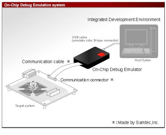
The RTE900/H1 On-Chip Debug Emulation System consists of Integrated Development Environment, RTE900/H1 On-Chip Debug Emulator and a communication cable. It provides various debug functions by controlling the on-chip debug function of the microcomputer mounted onto the target system.
- Capable of debugging in the operating condition equivalent to the MCU installed product.
- Real-time PC/PD trace.
- Trace control using an event feature.
- Capable of referring to the memory during program execution.
| Host interface | USB2.0 High-speed | |
|---|---|---|
| Emulation memory | Target memory | |
| Event | Number of points | 8 points |
| Comparison items | Address, data, status, external input | |
| Comparison conditionscondition | Match, unmatch, range | |
| Pass count | 1 to 256 times | |
| Event trigger actions | Break, trace control, timer control, external trigger output | |
| Event combinations | AND, OR, sequential | |
| Hardware break | 4 points | |
| Software break | 1024 points | |
| Trace memory Capacity | 256 frames (Notes-1) | |
| Trace memory Modes | Free trace, trigger trace, sampling trace | |
| Trace items | PC address, data address, data value, status, external output, external input, event | |
| Trace overflow actions | Overwriting, overwriting prohibit, break | |
| Timer measurement | Run timer: 1 channel, Lap timer: 1 channel | |
| Memory access | Memory display during program execution | 64 bytes |
| Memory rewrite during program execution | 1 address(byte/word/Long word either) (Notes-2) | |
| Program variables | Display | Binary, octal, decimal or hexadecimal display can be selected for each variable. |
| Registration | Variables, arrays, structures and unions can be registered by the elements. | |
| Sauce display | - Source - Source + assembler code - Source + assembler code + machine language |
|
| External output | 1 line | |
| External input | 1 line | |
| Performance analysis: Module time measurement | - | |
| Performance analysis: Coverage measurement | - | |
| Flash programming/security feature | External Flash memory can be programmed during debugging. | |
(Notes-1) There are some cases where the trace memory capacity varies by a tracing condition or operating status.
(Notes-2) A break occurs whenever rewritten.
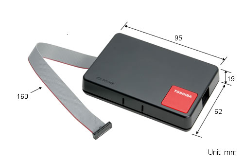
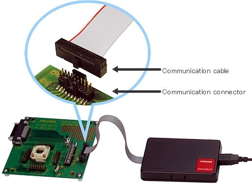
Product Configuration and Appearance of RTE900/H1 On-Chip Debug Emulator
Content of Product
- RTE900/H1 On-Chip Debug Emulator main body
- Communication cable (already connected to the emulator main body) (Notes)
- Communication connector (Notes)
- One license for downloading the Integrated Development Environment from website.
(Notes) Made by Samtec,Inc.
Items to Be Prepared by Customer
- Host system
- USB cable (emulator side: B-type connector)
- Microcomputer on the target system (with on-chip debug function incorporated)
About Connection to Target System
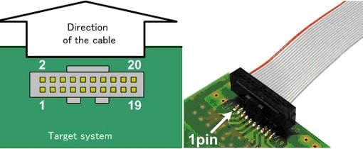
Seeing the following pin assignment table, etc., lay out/mount the Communication Connector (FTSH series 20pin connector made by Samtec, Inc.) on to the target system where the On-chip debug emulation system is to be connected.
One Communication Connector comes with an emulator, but those of the identical series (FTSH series) released from Samtec, Inc. are also available.
FTSH-110-01-[*]-[*][*]-[*][*]
[*] of the part number indicates a connector option. When purchasing, choose a suitable option according to its usage. For details specifications, please visit Samtec, Inc. website.
Communication Connector attached to an Emulator
| Part Nnumber |
Note |
|---|---|
| FTSH-110-01-L-DV-K | Surface mount type with keying shroud |
Communication Connector Pin Assignment Table
| Connector Pin No. | Signal Name |
|---|---|
| 1 | EI_SYNCLK |
| 3 | EO_MCUDATA |
| 5 | EI_PODDATA |
| 7 | EO_MCUREQ |
| 9 | EI_PODREQ |
| 11 | N.C (notes-1) |
| 13 | N.C (notes-1) |
| 15 | EI_REFCLK |
| 17 | EO_COMRESET |
| 19 | DVCC3A |
| Connector Pin No. | Signal Name |
|---|---|
| 2 | GND |
| 4 | GND |
| 6 | GND |
| 8 | GND |
| 10 | GND |
| 12 | GND |
| 14 | GND |
| 16 | GND |
| 18 | GND |
| 20 | DVCC3A |
(Notes-1)
(Notes) For the MCU pin numbers, signal names and connection method, be sure to see a data sheet for the target MCU.
Note for Layout of Communication Cable Connector
To monitor the waveforms of the EI_TRGIN and EO_TRGOUT signals, prepare external I/O pins on the target system as required. The following figure shows the cable pull-out direction and connector pin position, when the emulator is connected. To design the board, take into account interference with other parts at the time of connecting the communication cable. For a connector size, please visit Samtec, Inc. website.
Points of concern in signal wiring
To monitor the waveforms of the EI_TRGIN and EO_TRGOUT signals, prepare external I/O pins on the target system as required.
Each debug communication signal should be connected by locating the communication cable connecor within 10 cm (4 inches) from the MCU. Especially, the EI_SYNCLK, EO_MCUDATA, EI_PODDATA, EO_MCUREQ and EI_PODREQ signals must be connected with the same length of wire. If the wire length is longer than 10 cm, or it varies greately among these signals, proper operation may not be obtained.
All the DVCC3A and GND lines between the MCU and the communication cable connector should be as short as possible (preferably within 5 cm, within 10 cm at the longest). If the DVCC3A and GND lines are long, proper operation may not be ontained.
The communication connector should be connected directly to the MCU pattern. If a dumping resistor is inserted between the MCU and the communication cable connector, be careful of signal delays.
About Emulation Operating Voltage/Frequency
- Any operating Voltage/Frequency in the device operation assurance range is available.
- Note that the power/clock cannot be supplied from the emulator to the target system.
Limitation of the On-Chip Debug Emulation
- When connecting an on-chip debug emulator to a debug target system, communication pins and monitor pins are not available as a combined feature because they are occupied by the emulator.
- For the operation assurance range and characteristics of the supplied power/clock, see the microcomputer's datasheet.
Precautions for USB Connection
- The emulator is connected to the host system via the USB. (USB2.0 High-speed)
- To newly connect the emulator to the host system, it is necessary to install a USB driver.
Accessory
Communication Cable
The communication cable is used to connect the emulator or the FLASH Writer to the target system. It is pre-plugged to the emulator or the FLASH Writer.
The communication cable is available from Samtec, Inc. For detailed specifications, please visit Samtec, Inc. website.
The recommended product can also be purchased from the following agencies.
| Name | Part Number | Remark |
|---|---|---|
| Communication cable | FFSD-10-D-07.00-01-N | Pre-plugged to the emulator or the FLASH Writer |
Communication Connector
The communication connector is used to connect the emulator or the FLASH Writer to the target system. The part numbers shown below are examples. Other mount types, such as through-hole, and other mating options are also available to meet the specific needs of each customer.
The communication connector is available from Samtec, Inc. For detailed specifications, please visit Samtec, Inc. website.
The recommended product can also be purchased from the following agencies.
| Name | Part Number | Remark |
|---|---|---|
| Communication connector | FTSH-110-01-L-DV-K | Surface mount type with keying shroud. Each emulator comes with one communication connector. |