- 半導體首頁
-
應用Automotive
Body Electronics
xEV
In-Vehicle Infotainment
Advanced Driver-Assistance Systems (ADAS)
Chassis
IndustrialInfrastructure
BEMS/HEMS
Factory Automation
Commercial Equipment
Consumer/PersonalIoT Equipment
Healthcare
Wearable Device
Mobile
Computer Peripherals
-
產品車用元件
Discrete Semiconductor
Diodes
電晶體
通用邏輯IC
Analog Devices
Digital Devices
Wireless Devices
※
: Products list (parametric search)
功率半導體※
: Products list (parametric search)
隔離器/固態繼電器Photocouplers
Digital Isolators
※
: Products list (parametric search)
MOSFETsIGBTs/IEGTs雙極性電晶體※
: Products list (parametric search)
Diodes※
: Products list (parametric search)
微控制器馬達驅動 ICs智能功率 ICs※
: Products list (parametric search)
電源管理 ICs線性 ICs※
: Products list (parametric search)
通用邏輯 ICs線性影像感測器其他產品其他產品
※
: Products list (parametric search)
-
開發/設計支援
開發 / 設計支援
-
技術知識
- 購買管道
- 型號 & 關鍵字搜尋
- 交叉搜尋
- 參數搜尋
- 線上庫存查詢跟購買
This webpage doesn't work with Internet Explorer. Please use the latest version of Google Chrome, Microsoft Edge, Mozilla Firefox or Safari.
型號需要超過三個文字以上 Search for multiple part numbers fromhere.
The information presented in this cross reference is based on TOSHIBA's selection criteria and should be treated as a suggestion only. Please carefully review the latest versions of all relevant information on the TOSHIBA products, including without limitation data sheets and validate all operating parameters of the TOSHIBA products to ensure that the suggested TOSHIBA products are truly compatible with your design and application.Please note that this cross reference is based on TOSHIBA's estimate of compatibility with other manufacturers' products, based on other manufacturers' published data, at the time the data was collected.TOSHIBA is not responsible for any incorrect or incomplete information. Information is subject to change at any time without notice.
型號需要超過三個文字以上
1-1. Energy band diagram
Free electrons in a material allow a free flow of electricity. Although being part of atoms, free electrons are so loosely bound to atoms in a material, they can move about freely.
In classical physics, the Bohr model is a physical model that consists of a small atomic nucleus of protons and neutrons around which electrons travel in multiple orbits. Each element has a fixed number of electrons, which are placed from the orbit closest to the nucleus. For example, silicon (Si), a semiconductor, has 14 electrons. Figure 1-3 shows the Bohr model of silicon.
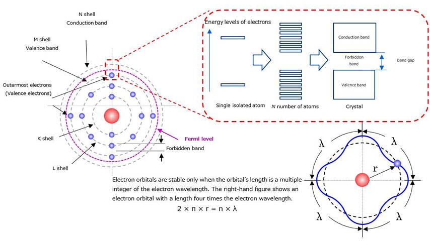
Since electrons have a wave nature, they are stable only on an orbital with a radius that is an integer multiple of their wavelength. Therefore, electrons move in discrete orbitals as represented by the Bohr model.
The electron orbital in a single isolated atom has an extremely narrow energy band. However, according to the Pauli exclusion principle, two or more electrons cannot occupy the same orbital. Therefore, as the state of matter changes from a single atom to a molecule to a crystal, their electron orbitals come to form a continuous band structure of energy levels
The closer the electrons are to the nucleus, the more tightly bound they are to the nucleus. The most loosely bound electrons in the outermost shell are called valence electrons. This outermost shell is called the valence band. The area beyond the outermost shell is called the conduction band. Since electrons have a wave nature as described above, there is an energy gap between the valence and conduction bands where electrons cannot exist. This energy gap is called a forbidden band.
Electrons in a valence band cannot move freely since they are bound to the nucleus. For these electrons to move freely between atoms, they have to absorb enough heat or light energy to be excited from the valence band to the conduction band (e.g., from the M shell to the N shell). The minimum amount of energy required for this electron excitation is the band gap.
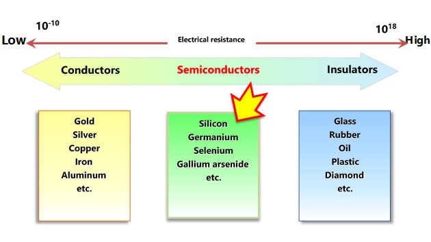
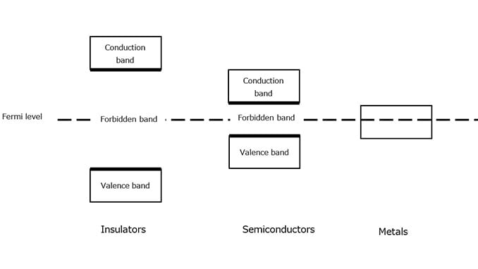
Figure 1-4 shows the energy bands of insulators, semiconductors, and metals.
In the case of insulators and semiconductors, the outermost shell occupied by electrons is called the valence band, and the shell that is not populated by any electrons is called the conduction band. In the case of metals, not all the orbitals in the outermost conduction band are populated by electrons. Because metals have empty orbitals, electrons are free to move in metals.
The valence and conduction bands are separated by a forbidden band where electrons cannot exist in a stable state. The energy width of the forbidden band is called a band gap. Semiconductors have a narrower forbidden band (i.e., smaller band gap) than insulators.
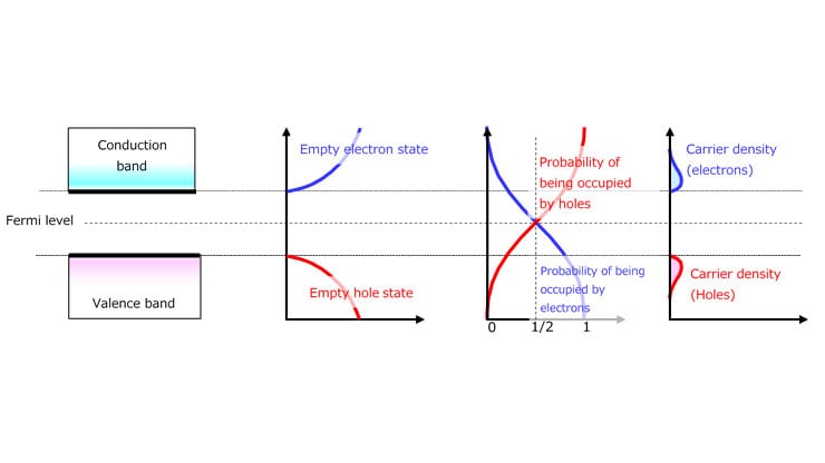
Insulators and semiconductors have a Fermi level between the conduction and valence bands. In the case of metals, the Fermi level is in the band where the energy level of the electrons that contribute to conduction is located. Although the Fermi level is defined as the energy level at which an orbital has a 50% probability of being occupied by electrons at any given time, the Fermi level of insulators and semiconductors falls in the forbidden band where no electrons exist.
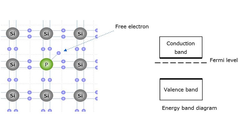
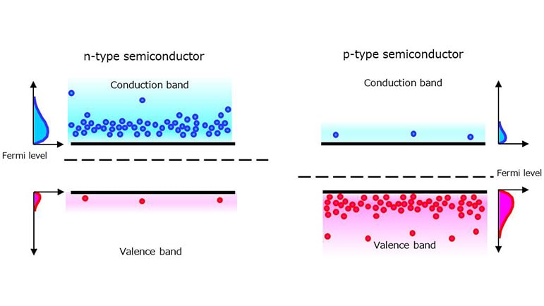
The following paragraphs describe n-type and p-type semiconductors that are created by adding impurities (called dopants) such as phosphor (P) and boron (B) to an intrinsic semiconductor, i.e., an undoped (pure) semiconductor.
n-type semiconductor:
Silicon has a valence of 4 with four bonding hands. It is an intrinsic semiconductor without any dopants or impurities. Let us see what occurs when the silicon crystal is doped with a valence of 5 elements (phosphorus (P), arsenic (As), or antimony (Sb)). Figure 1-5 shows that the phosphorus atom is able to bond with four silicon atoms, but since it has five valence electrons to offer, the fifth valence electron is left with nothing to bond to. Therefore, only a small amount of energy causes the fifth valence electron to be released as a free electron. Since the n-type semiconductor has extra electrons, its Fermi level approaches the conduction band at room temperature.
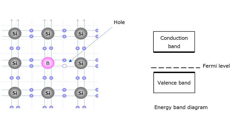
To create a p-type silicon semiconductor, a valence of 3 elements (boron (B), indium (In), or gallium (Ga)) is used as a dopant. Since a valence of 3 elements has only three electrons in the valence band, it attracts an electron from a silicon atom. The resulting empty bond site is called a hole, which is free to move in the silicon crystal just like free electrons. Since the p-type semiconductor has extra holes, its Fermi level approaches the valence band at room temperature.
Chapter1 Basics of Schottky Barrier Diodes (Basic of Semiconductor Device)
Related information
- Products
Schottky Barrier Diodes - Applidcation Notes
Application Notes - FAQs
Diodes - Parametric Search
Schottky Barrier Diodes - Stock Check & Purchase
Stock Check & Purchase


