
- 半導體首頁
-
應用Automotive
Body Electronics
xEV
In-Vehicle Infotainment
Advanced Driver-Assistance Systems (ADAS)
Chassis
IndustrialInfrastructure
BEMS/HEMS
Factory Automation
Commercial Equipment
Consumer/PersonalIoT Equipment
Healthcare
Wearable Device
Mobile
Computer Peripherals
-
產品車用元件
Discrete Semiconductor
Diodes
電晶體
通用邏輯IC
Analog Devices
Digital Devices
Wireless Devices
※
 : Products list (parametric search)功率半導體
※
: Products list (parametric search)隔離器/固態繼電器Photocouplers
Digital Isolators
※
: Products list (parametric search)MOSFETsIGBTs/IEGTs雙極性電晶體※
: Products list (parametric search)Diodes※
: Products list (parametric search)微控制器馬達驅動 ICs智能功率 ICs※
: Products list (parametric search)電源管理 ICs線性 ICs※
: Products list (parametric search)通用邏輯 ICs線性影像感測器其他產品其他產品
※
: Products list (parametric search) -
開發/設計支援
開發 / 設計支援
-
技術知識
- 購買管道


- 型號 & 關鍵字搜尋
- 交叉搜尋
- 參數搜尋
- 線上庫存查詢跟購買
This webpage doesn't work with Internet Explorer. Please use the latest version of Google Chrome, Microsoft Edge, Mozilla Firefox or Safari.
型號需要超過三個文字以上 Search for multiple part numbers fromhere.
The information presented in this cross reference is based on TOSHIBA's selection criteria and should be treated as a suggestion only. Please carefully review the latest versions of all relevant information on the TOSHIBA products, including without limitation data sheets and validate all operating parameters of the TOSHIBA products to ensure that the suggested TOSHIBA products are truly compatible with your design and application.Please note that this cross reference is based on TOSHIBA's estimate of compatibility with other manufacturers' products, based on other manufacturers' published data, at the time the data was collected.TOSHIBA is not responsible for any incorrect or incomplete information. Information is subject to change at any time without notice.
型號需要超過三個文字以上
What is a reverse-conducting IGBT (RC-IGBT)?
Back electromotive force is generated when controlling the on/off of an inductive load (such as a motor or coil) in an inverter or converter circuit. When using an IGBT for this on/off control, a freewheeling diode (FWD*1) connected in inverse parallel to the IGBT as shown in Fig. 1 is required to process the back electromotive force. A reverse conducting IGBT (RC-IGBT) is a product that combines an IGBT and FWD on a single chip.


An inductor, which is an inductive load, has the characteristic of generating a back electromotive force (reverse voltage) in response to changes in the load current, preventing changes in the current. In inverter and converter circuits, switching operations that turn inductive loads on and off are repeated. Normally, the on/off transition occurs very quickly, so the back electromotive force is very large. During the transition from on to off, a voltage exceeding the power supply voltage is applied to the IGBT, which may destroy the IGBT.
The load current generated by this back electromotive force is commutated in the reverse direction of the IGBT (from emitter to collector) through the FWD (freewheeling diode) connected in reverse parallel to the IGBT. Fig. 2 shows a circuit in which IGBTs with parallel-connected FWDs are arranged in series as one arm of an H-bridge circuit. When Q2 is turned off, the collector current IC that flows when Q2 is on generates a voltage that exceeds the collector voltage of Q1 due to the back electromotive force generated by the inductive load, causing the FWD to conduct and the current to be commutated.
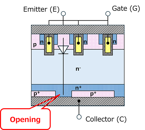
RC-IGBT is a single chip that incorporates this FWD. Fig. 3 shows the internal structure of RC-IGBT. The FWD has an opening in the p+ layer, which is the collector of the IGBT chip, connecting the n+ and collector terminals. This forms a PIN diode (n⁺–n⁻–p⁺ structure) between the emitter and collector electrodes, connected in anti-parallel with the IGBT. RC-IGBTs are used in soft switching applications such as ZVS (Zero Voltage Switching), and more recently have begun to be used in hard switching applications such as inverter circuits. However, due to trade-offs (such as the on-voltage of the IGBT and the reverse recovery time of the FWD), it is difficult to optimize both performances, so compatibility must be confirmed for applications that place importance on high-speed performance or forward characteristics.
Please refer to the following FAQ for information on IGBT on-voltage.
Please refer to the following FAQ for information on soft switching such as ZVS.
Please refer to the following FAQ for information on FWD reverse recovery time.
*1: FWD: An abbreviation for Free Wheeling Diode. It is used as a path (commutation path) for the back electromotive force generated in the reactance load.
*2: PIN diode: A diode that has a high-resistance I layer (intrinsic layer: close to an intrinsic semiconductor, with a low impurity concentration and high resistance) sandwiched between a P layer and an N layer. This structure is used for the FWD of IGBTs, which require high withstand voltages.
相關信息
The following documents also contain related information.
參數搜尋
IGBTs/IEGTs
常見問答
* Company names, product names, and service names used in this FAQ may be of their respective companies.