
- 半導體首頁
-
應用Automotive
Body Electronics
xEV
In-Vehicle Infotainment
Advanced Driver-Assistance Systems (ADAS)
Chassis
IndustrialInfrastructure
BEMS/HEMS
Factory Automation
Commercial Equipment
Consumer/PersonalIoT Equipment
Healthcare
Wearable Device
Mobile
Computer Peripherals
-
產品車用元件
Discrete Semiconductor
Diodes
電晶體
通用邏輯IC
Analog Devices
Digital Devices
Wireless Devices
※
 : Products list (parametric search)功率半導體
※
: Products list (parametric search)隔離器/固態繼電器Photocouplers
Digital Isolators
※
: Products list (parametric search)MOSFETsIGBTs/IEGTs雙極性電晶體※
: Products list (parametric search)Diodes※
: Products list (parametric search)微控制器馬達驅動 ICs智能功率 ICs※
: Products list (parametric search)電源管理 ICs線性 ICs※
: Products list (parametric search)通用邏輯 ICs線性影像感測器其他產品其他產品
※
: Products list (parametric search) -
開發/設計支援
開發 / 設計支援
-
技術知識
- 購買管道


- 型號 & 關鍵字搜尋
- 交叉搜尋
- 參數搜尋
- 線上庫存查詢跟購買
This webpage doesn't work with Internet Explorer. Please use the latest version of Google Chrome, Microsoft Edge, Mozilla Firefox or Safari.
型號需要超過三個文字以上 Search for multiple part numbers fromhere.
The information presented in this cross reference is based on TOSHIBA's selection criteria and should be treated as a suggestion only. Please carefully review the latest versions of all relevant information on the TOSHIBA products, including without limitation data sheets and validate all operating parameters of the TOSHIBA products to ensure that the suggested TOSHIBA products are truly compatible with your design and application.Please note that this cross reference is based on TOSHIBA's estimate of compatibility with other manufacturers' products, based on other manufacturers' published data, at the time the data was collected.TOSHIBA is not responsible for any incorrect or incomplete information. Information is subject to change at any time without notice.
型號需要超過三個文字以上
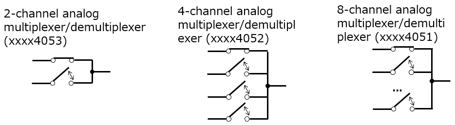
Sequential Logic: Shift Registers
Shift registers
Examples: 74VHC164, 74VHC165
Shift registers can be configured for serial-parallel (SI-PO) or parallel-serial (PI-SO) conversion.
Parallel-serial conversion helps reduce the number of transmission lines (i.e., transmission bit width). Some shift registers have the CLR input that is used to initialize the internal state to a known value.
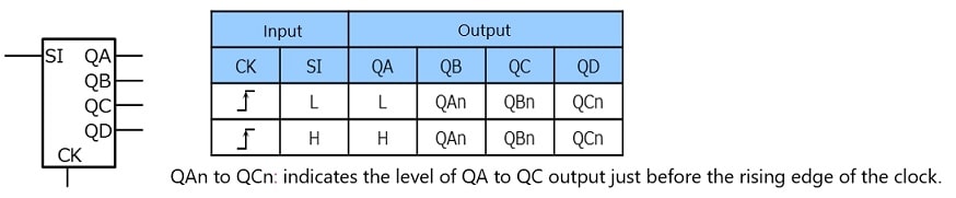
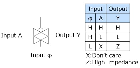
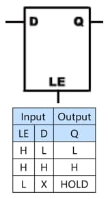
The following shows the logic symbol and truth table of a shift register.
A shift register is composed of multiple flip-flops.
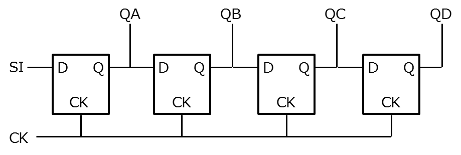
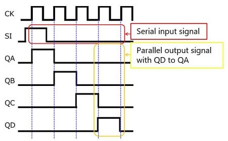
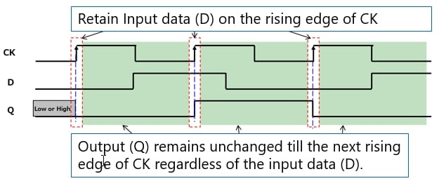
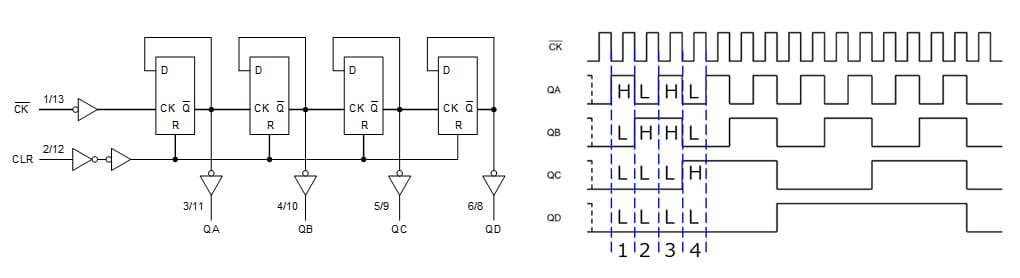
Operation of a shift register
The following describes the operation of a shift register using a logic schematic and a timing diagram. A shift register is composed of a cascade of flip-flops in which the output (Q) of each flip-flop is connected to the data (D) input of the next flip-flop in the chain.
A serial input (SI) is applied to the data (D) input of the first flip-flop. The data from SI are latched on the rising edge of the clock (CK) and appear at QA. With four clock pulses, the data from SI are transferred to the fourth flip-flop. As a result, the serial input (SI) is converted to parallel output data appearing at QD, QC, QB, and QA.
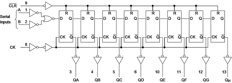
Types of shift registers
Logic schematic of the 74VHC164 eight-bit SI-PO shift register

Logic schematic of the 74VHC165 eight-bit PI-SO shift register
There are serial-in/parallel-out and parallel-in/serial-out shift registers.
- Prev
- 12/12
Chapter3 Basic CMOS Logic ICs


Products
Related information
- Application Notes
- FAQ