
- 半導體首頁
-
應用Automotive
Body Electronics
xEV
In-Vehicle Infotainment
Advanced Driver-Assistance Systems (ADAS)
Chassis
IndustrialInfrastructure
BEMS/HEMS
Factory Automation
Commercial Equipment
Consumer/PersonalIoT Equipment
Healthcare
Wearable Device
Mobile
Computer Peripherals
-
產品車用元件
Discrete Semiconductor
Diodes
電晶體
通用邏輯IC
Analog Devices
Digital Devices
Wireless Devices
※
 : Products list (parametric search)功率半導體
※
: Products list (parametric search)隔離器/固態繼電器Photocouplers
Digital Isolators
※
: Products list (parametric search)MOSFETsIGBTs/IEGTs雙極性電晶體※
: Products list (parametric search)Diodes※
: Products list (parametric search)微控制器馬達驅動 ICs智能功率 ICs※
: Products list (parametric search)電源管理 ICs線性 ICs※
: Products list (parametric search)通用邏輯 ICs線性影像感測器其他產品其他產品
※
: Products list (parametric search) -
開發/設計支援
開發 / 設計支援
-
技術知識
- 購買管道


- 型號 & 關鍵字搜尋
- 交叉搜尋
- 參數搜尋
- 線上庫存查詢跟購買
This webpage doesn't work with Internet Explorer. Please use the latest version of Google Chrome, Microsoft Edge, Mozilla Firefox or Safari.
型號需要超過三個文字以上 Search for multiple part numbers fromhere.
The information presented in this cross reference is based on TOSHIBA's selection criteria and should be treated as a suggestion only. Please carefully review the latest versions of all relevant information on the TOSHIBA products, including without limitation data sheets and validate all operating parameters of the TOSHIBA products to ensure that the suggested TOSHIBA products are truly compatible with your design and application.Please note that this cross reference is based on TOSHIBA's estimate of compatibility with other manufacturers' products, based on other manufacturers' published data, at the time the data was collected.TOSHIBA is not responsible for any incorrect or incomplete information. Information is subject to change at any time without notice.
型號需要超過三個文字以上
Countermeasures for Latch-Up
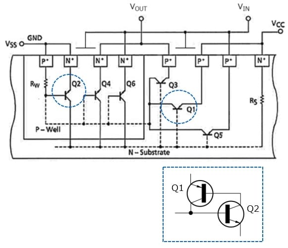
A latch-up is a phenomenon specific to CMOS integrated circuits that is caused by SCR (Silicon Controlled Rectifier) generation.
Let’s consider a CMOS logic IC formed on an n-substrate. A CMOS logic IC has various parasitic bipolar transistors (Q1 to Q6), internally forming a triac circuit. A common cause of a latch-up is excessive noise, surge voltage, or surge current on an input or output pin of a CMOS IC. Another cause is a sharp change in the supply voltage. In such cases, the internal triac circuit turns on, causing an excessive current to continue flowing between VCC and GND even if the triggering signal is disconnected, and eventually leading to the destruction of the IC.
The following briefly describes the process leading to a latch-up.
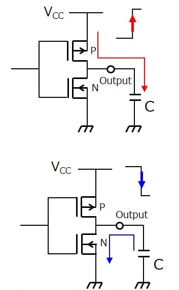
The below figure shows an equivalent circuit of a CMOS circuit, including its parasitic structure. An NPN transistor (Q2) is formed in the p-well on the n-channel MOSFET side while a PNP transistor (Q1) is formed in the n-substrate on the p-channel MOSFET side. Parasitic resistances (RS and RW) also exist between IC pins. Parasitic elements (Q1 and Q2) form a thyristor.
For example, if current flows into the n-substrate because of an external cause, a voltage drop occurs across resistor RS in the n-substrate. As a result, Q1 turns on, causing current to flow from VCC to GND via resistor RW in the p-well. The current flowing through RW produces a voltage difference across RW, which turns on Q2, causing supply current to flow via RS. Since this further increases the voltage difference across RS, Q1 and Q2 remain on. Consequently, the supply current continues increasing. As described above, CMOS ICs suffer from a latch-up problem when voltage differences occur across RW in the p-well and RS in the n-substrate.

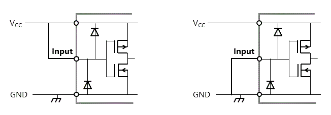
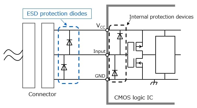
Countermeasure for latch-up
Use under the rated conditions.
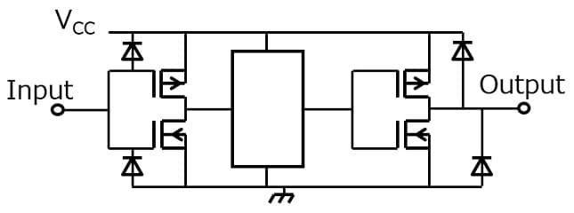
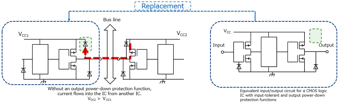
But it is recommended to add a protection circuit to the IC interface as shown in below figure.
if an excessive surge might be applied to the IC.
CMOS邏輯IC的使用注意事項


Products
Related information
- Application Notes
- FAQ