
-
My ToshibaSemicon
- セミコンダクタートップ
-
アプリケーション車載
ボディエレクトロニクス
xEV
インフォテインメント
産業用機器業務用機器
民生/個人用機器 -
製品車載用デバイス
ディスクリート半導体
ダイオード
トランジスター
汎用ロジックIC
アナログデバイス
※
 : 製品一覧(パラメトリックサーチ)パワー半導体
※
: 製品一覧(パラメトリックサーチ)アイソレーター/ソリッドステートリレー(SSR)フォトカプラー
デジタルアイソレーター
ソリッドステートリレー (SSR)
光伝送モジュール
※
: 製品一覧(パラメトリックサーチ)MOSFETIGBT/IEGTバイポーラートランジスター※
: 製品一覧(パラメトリックサーチ)ダイオード※
: 製品一覧(パラメトリックサーチ)マイクロコントローラーモータードライバーインテリジェントパワーIC※
: 製品一覧(パラメトリックサーチ)パワーマネージメントICリニアーIC※
: 製品一覧(パラメトリックサーチ)汎用ロジックICリニアーイメージセンサーその他専用ICその他専用IC
※
: 製品一覧(パラメトリックサーチ) -
開発/設計支援
-
知る/学ぶ
- ご購入


- 品番・キーワード検索
- クロスリファレンス検索
- パラメトリック検索
- オンラインディストリビューター在庫検索
本機能は Internet Explorer 11 ではご利用頂けません。最新のGoogle Chrome, Microsoft Edge, Mozilla Firefox, Safariにてご利用ください。
品番は3文字以上指定して下さい。 複数品番の検索はこちら。
クロスリファレンスでは参考品名が表示されますので、製品に関する最新の情報をデータシート等でご確認の上、単独およびシステム全体で十分に評価し、お客様の責任において適用可否を判断してください。参考にしている情報は、取得した時点の各メーカーの公式情報に基づいた当社の推定によるものです。当社は、情報の正確性、完全性に関して一切の保証をいたしません。また、情報は予告なく変更されることがあります。
品番は3文字以上指定して下さい。
オンラインディストリビューターが保有する東芝製品の在庫照会および購入が行えるサービスです。
産業用機器に適したゲート駆動電流を提供するMOSFET・IGBTゲート駆動用フォトカプラー
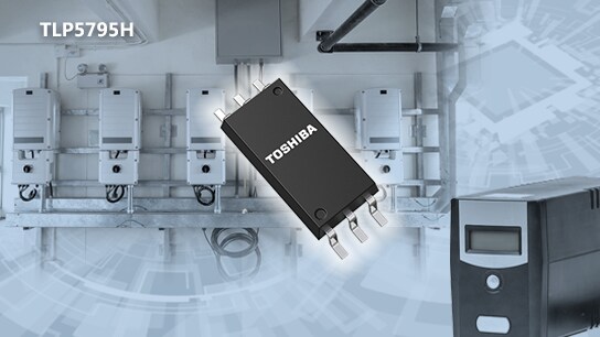
当社は、小~中容量のMOSFETやIGBTのゲート駆動向けに、フォトカプラー「TLP5795H」を製品化し、1A~5Aクラスのゲート駆動電流を提供するラインアップを拡充しました。
近年、グリーンエナジーやファクトリーオートメーション (FA) 市場の拡大に伴い、低電圧の制御側から高電圧のパワーデバイスへ絶縁を介して駆動する絶縁型ゲートドライバーの需要が増加しています。これらの市場において、絶縁型ゲートドライバーの駆動性能をより正確に把握する仕様の要求が高まっています。この要求に対して、当社は出力電流特性IOLH、IOHLを標準値として規定した-4.5/+5.3A (typ.) のTLP5795Hを製品化しました。さらに-6.0/+4.0A (typ.) のTLP5794H、-1.0/+1.0A (typ.) のTLP5791Hを開発しています[注1]。
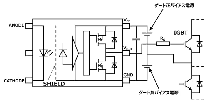
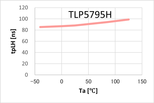
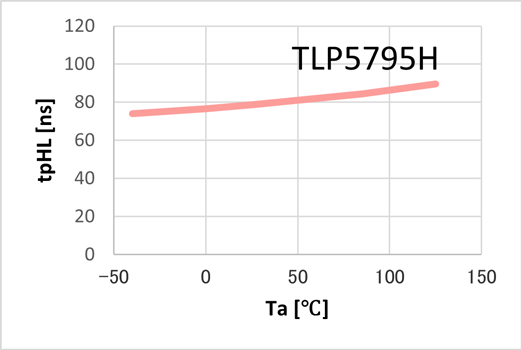
新製品TLP5795Hは、ピークハイレベル/ローレベル出力電流 (IOLH/IOHL) として-4.5/+5.3Aの性能を有し、UVLO[注2]スレッショルド (VUVLO+) は13.5V (max)、UVLOスレッショルド (VUVLO-) は11.1V (min)、UVLOヒステリシス (UVLOHYS) は1.0V (typ.) です。この仕様は、IGBTおよびゲート負バイアス電圧定格が広めのSiC MOSFETの駆動を想定しており、正バイアス15~20V、負バイアス0~-10V程度でのパワーデバイス駆動に適した仕様となっております。アプリケーションノート「ゲートドライバーカプラーパワーデバイス ゲート負バイアス電源使用時の注意事項」もご参考ください。伝搬遅延時間は温度依存性が少ないため、FA機器で定義されている実用域で安定した動作が可能です。また、TLP5795Hはレール・トゥ・レール[注3]出力品であり、電源電圧からの電圧ドロップが少ないスイッチング特性を可能にします。
さらに、入力側の赤外発光ダイオードの光出力向上と受光素子 (フォトダイオードアレイ) の最適化設計により光結合効率を高め、動作温度定格-40°Cから125°Cを実現しました。これにより、PVインバーター、UPS[注4]、EVスタンドなど、厳しい熱環境で使用される産業用機器に対応できます。伝搬遅延時間や伝搬遅延スキューも動作温度定格範囲で規格化しています。パッケージは小型SO6Lを採用し、セット基板上での部品配置の自由度向上に貢献します。さらに、最小沿面距離8.0mmを確保しており、絶縁耐圧は5000Vrmsなので高い絶縁性能を必要とする用途にも対応可能です。
今後も、当社は産業用機器向けMOSFET・IGBTゲート駆動用フォトカプラーの開発を進め、ラインアップを拡充してまいります。
[注1] TLP5794H、TLP5791Hは2025年6月製品化予定
[注2] Under Voltage Lock Outの略名。低電圧誤動作防止機能のこと。
[注3] 出力電圧が電源電圧の範囲全体 (正電源レールから負電源レールまで) をカバーできることを指す。低電圧で動作する回路や、電源電圧の範囲全体で信号を処理する必要があるアプリケーションにおいて有用。
[注4] UPS: Uninterruptible Power Supply (無停電電源装置)
新製品の主な特長
- SiC MOSFETに対応したUVLO: 13.5V (max)
- 安定した伝搬遅延時間
- レール・トゥ・レール出力[注3]
特長の解説
1. SiC MOSFETに対応したUVLO: 13.5V (max)
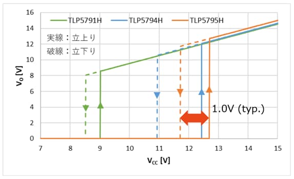
高いゲート電圧を設定できるため、高電力アプリケーションに適しています。また、ヒステリシスが1.0V (typ.) あることで出力が安定し、システム全体の信頼性が向上します。
2. 安定した伝搬遅延時間
伝搬遅延時間は、-40~125°Cの動作温度定格内で安定した動作をします。さらに、FA機器で定義されている実用域で安定した動作をします。
3. レール・トゥ・レール出力[注3]
レール・トゥ・レール出力により、電源電圧の範囲で出力電圧が使用できます。また、ゲートドライバーカプラーの内部抵抗が小さいため、低損失となります。これにより、スイッチング損失が最小限に抑えられ、機器の効率が向上します。
アプリケーション
- PVインバーター
- UPS
- EVチャージャースタンド
- インバータードライブ
- IHクッキング
- エアコン
新製品の主な仕様
(特に指定のない限り、Ta=-40~125°C)
品番 |
TLP5794H[注1] |
TLP5791H[注1] |
||||
|---|---|---|---|---|---|---|
パッケージ |
名称 |
|||||
寸法 (mm) |
Typ. |
3.84×10×2.1 |
||||
推奨動作条件 |
ピークハイレベル/ローレベル出力電流 (L/H) IOLH、(H/L) IOHL (A) |
-4.5/+5.3 |
-6.0/+4.0 |
-1/+1 |
||
電源電圧 VCC (V) |
15~30 |
15~30 |
10~30 |
|||
電気的特性 |
UVLOスレッショルド VUVLO+ (V) |
IF=5mA、 VO>2.5V |
Max |
13.5 |
13.5 |
9.5 |
UVLOスレッショルド VUVLO- (V) |
IF=5mA、 VO<2.5V |
Min |
11.1 |
9.5 |
7.5 |
|
UVLOヒステリシス UVLOHYS (V) |
- |
Typ. |
1.0 |
1.5 |
0.5 |
|
スイッチング特性 |
伝搬遅延時間 (L/H) tpLH、(H/L) tpHL (ns) |
VCC=30V |
Max |
150 |
200 |
500 |
コモンモード過渡耐性 CMH、CML (kV/μs) |
Ta=25°C |
Min |
±35 |
±50 |
±20 |
|
絶縁特性 |
絶縁耐圧 BVS (Vrms) |
Ta=25°C |
Min |
5000 |
||
在庫検索&Web少量購入 |
 |
- |
- |
|||
関連コンテンツ
ゲートドライバーカプラー パワーデバイス ゲート負バイアス電源使用時の注意事項 (PDF: 1,241KB)
ご購入、サンプルに関するお問い合わせ
オンラインディストリビューター在庫検索&Web少量購入
オンラインディストリビューターが保有する東芝製品の在庫照会および購入が行えるサービスです。
品番は3文字以上指定して下さい。
ここから先は、東芝デバイス&ストレージ株式会社およびその関係会社(以下、総称して「当社」 といいます。)の販売代理店様のウェブサイト(以下、「第三者ウェブサイト」といいます。)になります。第三者ウェブサイトを通したお取引は、各販売代理店様が定める取引条件に従っていただくことになりますのでご了承ください。本ウェブサイトからリンクしている第三者ウェブサイトは、それらを運営する各販売代理店様がその責任において管理するものであり、当社の管理下にはありません。本ウェブサイトとリンクしている事実をもって、当社が第三者ウェブサイトの内容を推奨していることを意味するものではありません。また、当社は第三者ウェブサイトの内容及びそれを通したお取引についていかなる責任も負うものではありませんので、お客様ご自身の責任でご利用ください。
* 社名・商品名・サービス名などは、それぞれ各社が商標として使用している場合があります。
* 本資料に掲載されている情報 (製品の価格/仕様、サービスの内容及びお問い合わせ先など) は、発表日現在の情報です。予告なしに変更されることがありますので、あらかじめご了承ください。