


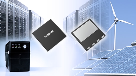
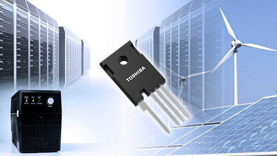
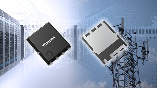
功率半導體
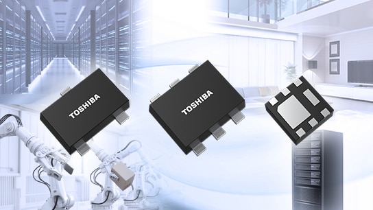
Semiconductor device that controls the flow of electricity to reduce power loss. Personal computers and other electronic equipment constantly lose power when they operate. Power loss can be kept low by using high performance power semiconductors. High performance power semiconductor can realize saving energy for not only Personal Computers, but also Smartphones, Automotive application, Trains, and Electrical substations.
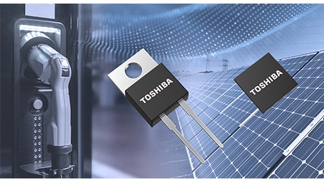
Sic功率元件
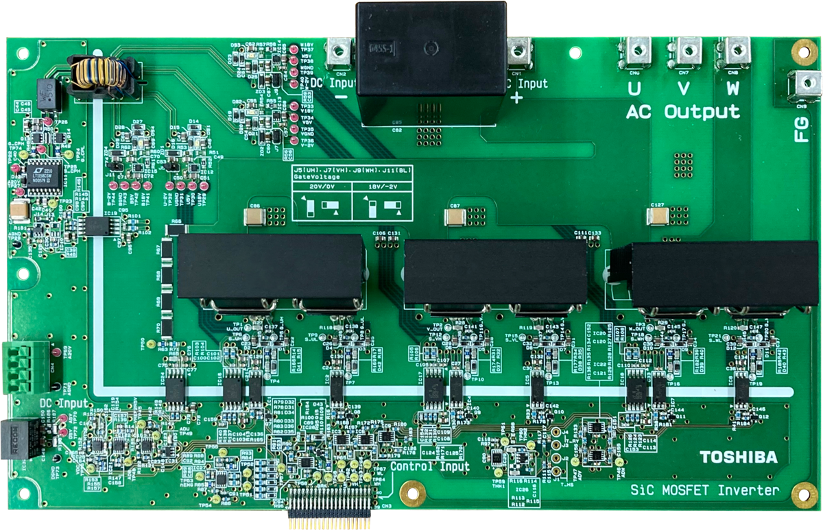
SiC MOSFETs
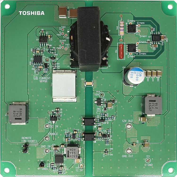
Toshiba’s 1200V SiC MOSFETs offers high-speed switching and low ON-resistance making it excellent for high-power, high-efficiency industrial power supplies, low-loss solar inverters and UPS.
SiC Schottky Barrier Diodes
Toshiba offers 650V products, 1200V products Silicon Carbide Schottky Barrier Diodes (SiC SBD) that achieve low forward voltage characteristics (VF).
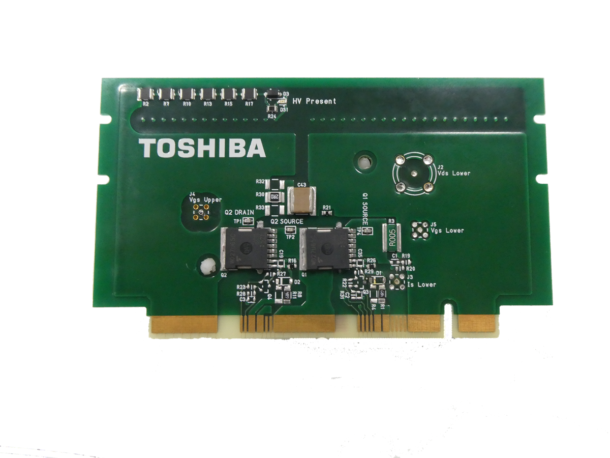
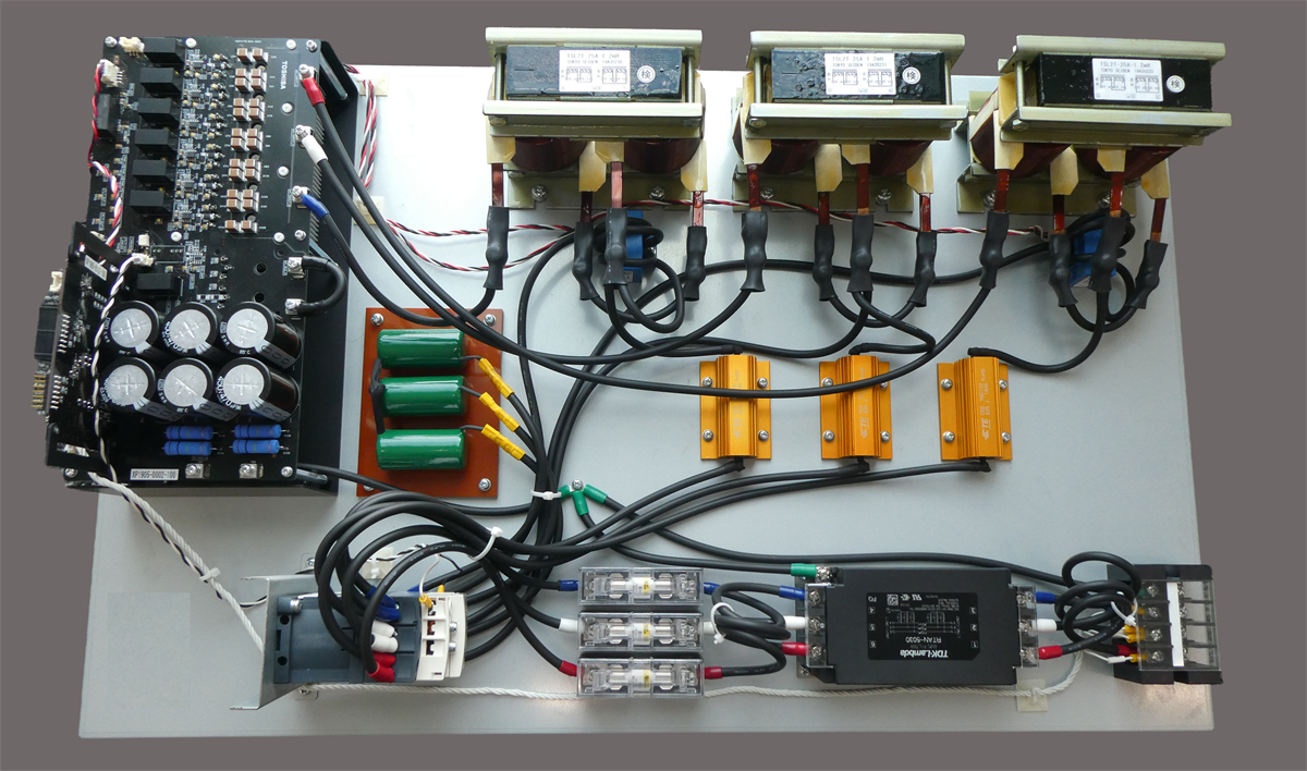
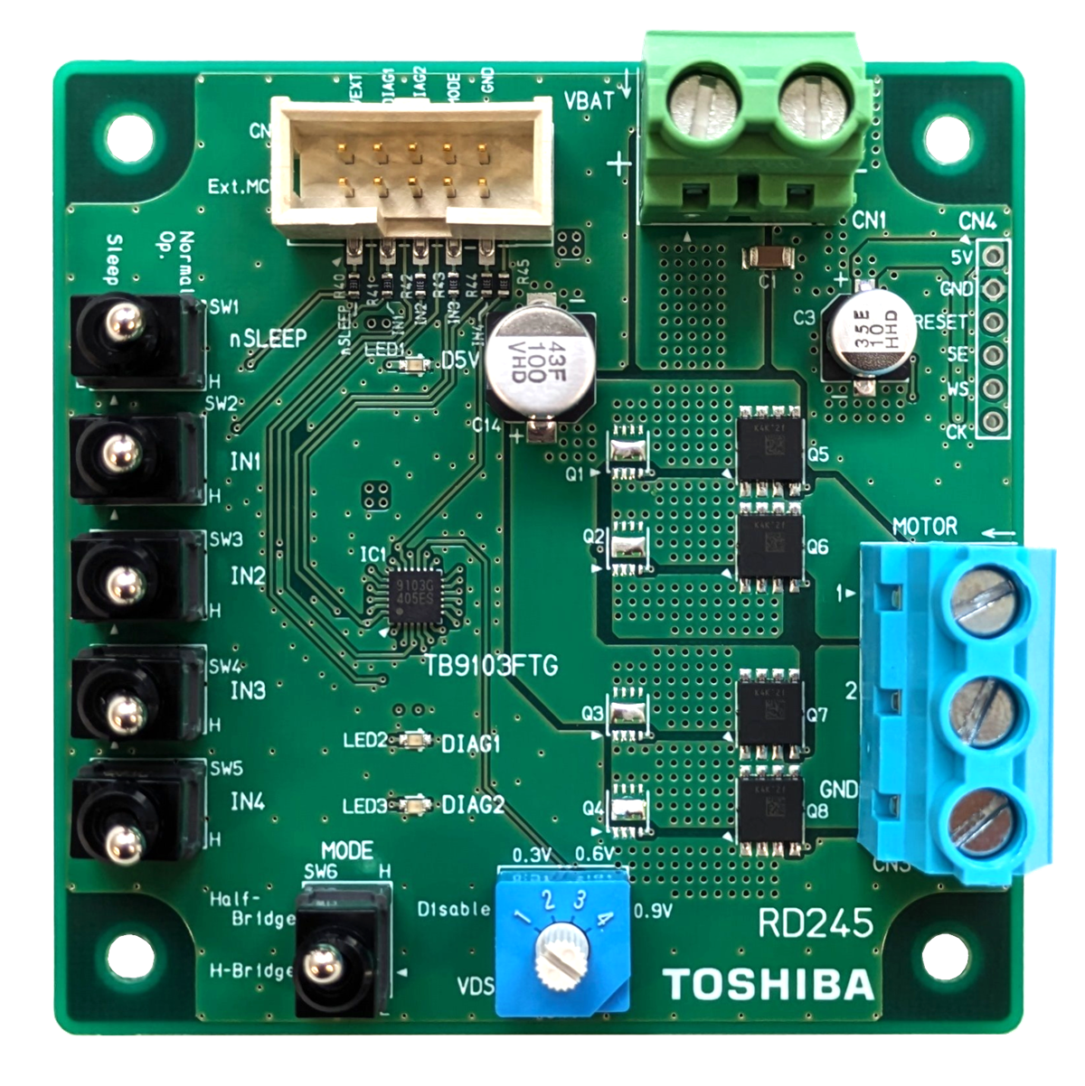
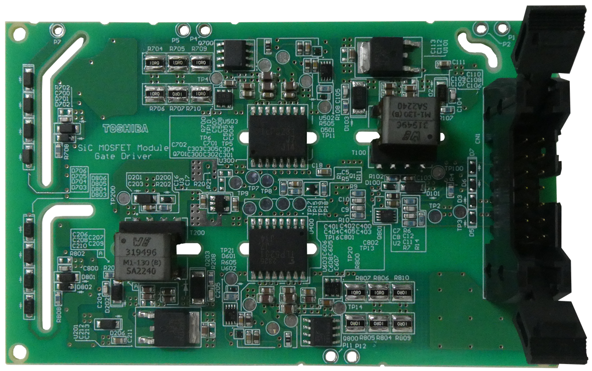
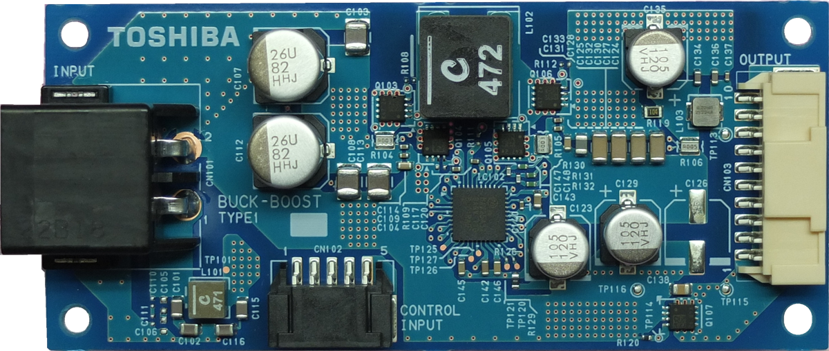
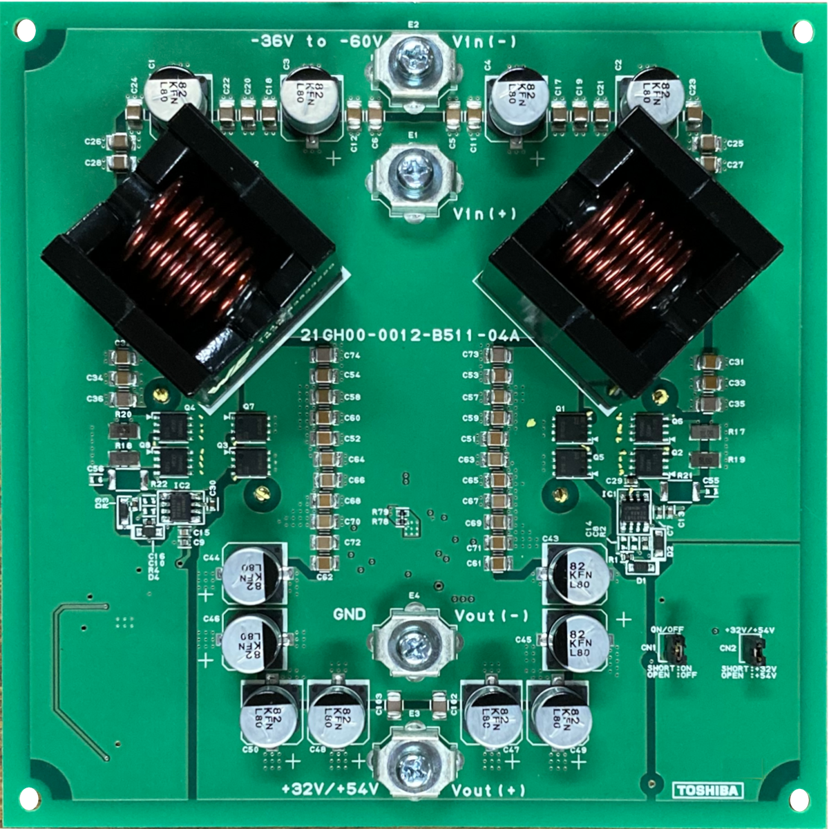
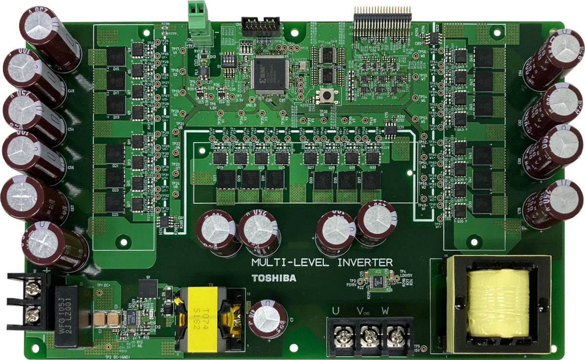
SiC MOSFETs Modules
Our SiC MOSFETs modules have high-speed switching properties, and use SiC (silicon carbide), a new material optimized for low-loss and miniaturization of power converters for the industry, such as inverters and converters for railway vehicles and photovoltaic inverters.
MOSFET
12V - 300V MOSFETs
Toshiba has used each successive generation of trench-gate structures and fabrication processes to steadily reduce the drain-source on-resistance, RDS(ON), of its low-voltage power MOSFETs.
400V - 900V MOSFETs
Toshiba offers super-junction MOSFET series suitable for high-output power supply applications and D-MOS (double-diffused) MOSFET series suitable for low-output power supply applications.
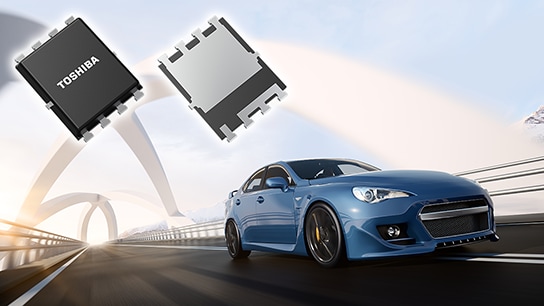
車用 MOSFETs
Toshiba offers an extensive line of power devices such as power MOSFETs for various automotive applications, including 12V battery and motor control systems.
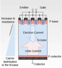
IGBTs/IEGTs
IGBTs
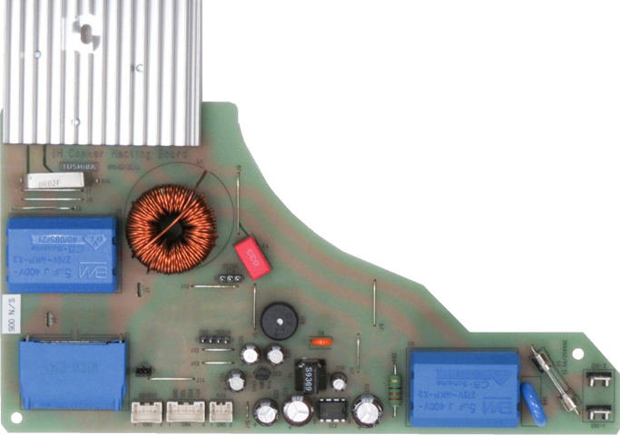
Toshiba discrete IGBTs contribute energy savings in applications, such as IH cooking equipment, rice cookers, kitchen microwaves, refrigerators, washing machines, air-conditioners.
IEGT (PPI)
The outstanding turn-off performance and the wide safe operating area of IEGTs make it possible to reduce the power consumption, shrink the size and improve the efficiency of equipment.
Diodes
Switching Diodes
Toshiba offers 1-circuit to 4-circuit products, with forward current ranging from 80 to 500 mA, in small surface-mount packages suitable for high-density board assembly.
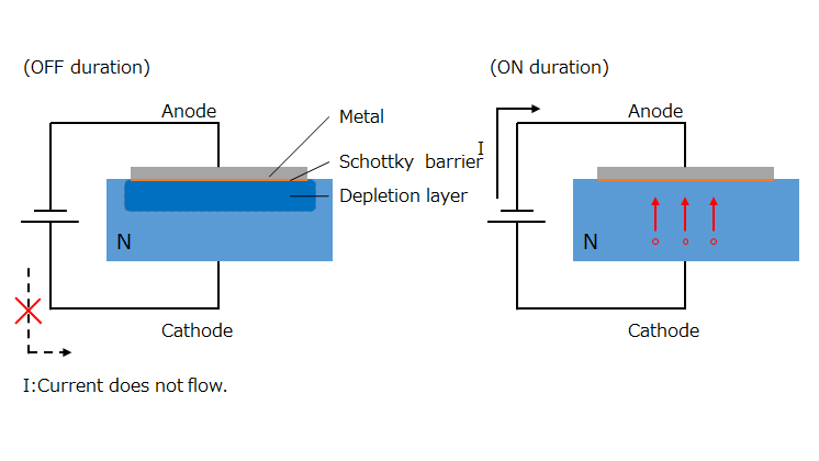
肖特基位障二極體
Toshiba offers superior low-VF and low-IR types ranging from general-purpose to power-line products. These can contribute to greater power efficiency and power saving.
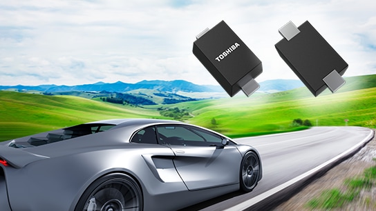
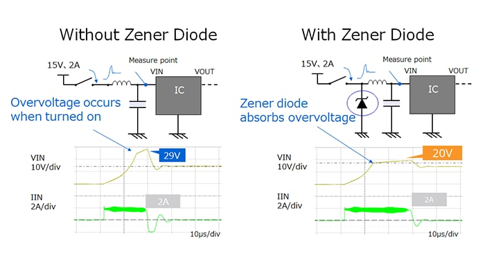
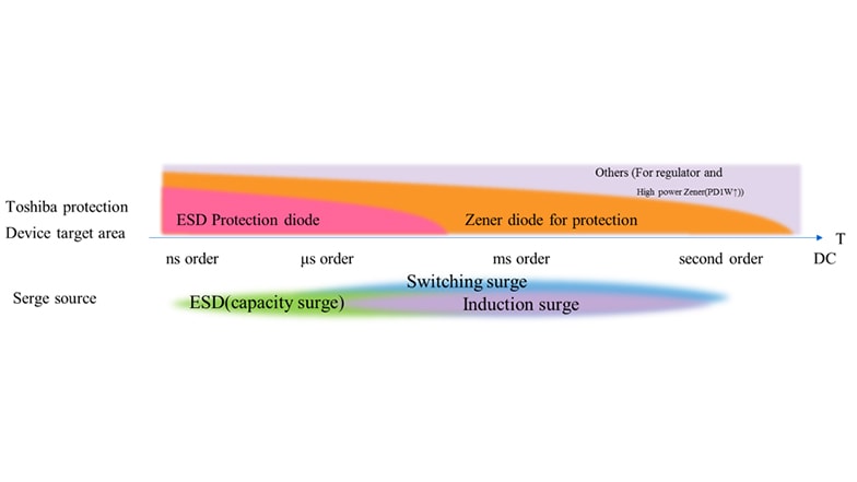
Zener Diodes
Zener diodes are available in a wide range of Zener voltage specifications extending from 5.6 V to 82 V. Their extensive application fields include both consumer and industrial electronics.
Rectifier Diodes
Diodes with reverse voltage ranging from 200 to 1000 V and an average forward current ranging from 0.5 to 3 A are offered in small and medium-size surface-mount packages.
雙極性電晶體
雙極性電晶體
Toshiba’s offers an extensive lineup ranging from ultra-small, surface-mounted, small-signal transistors to power transistors with lead-type packages, including low-saturation, high-current, and ultra-high-speed types.
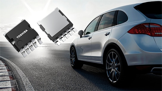
Automotive Bipolar Transistors
Toshiba’s extensive lineup ranges from ultra-small, surface-mounted, small-signal transistors to power transistors with medium-sized, surface-mount packages, including low-saturation and high-current types.
Technical Articles
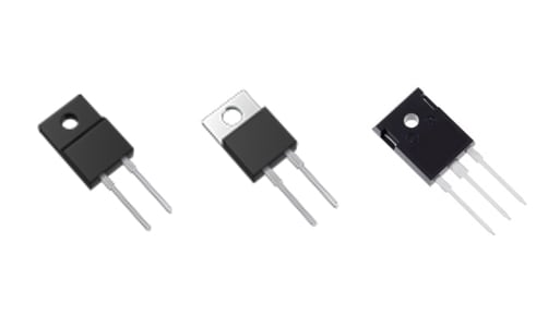
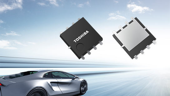
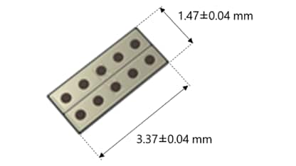
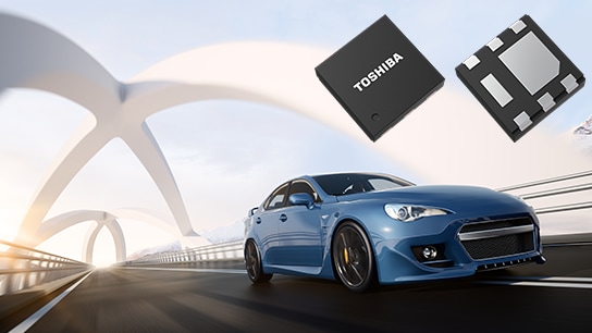
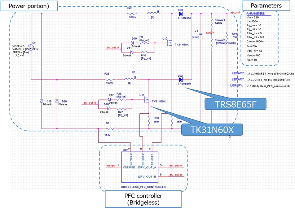
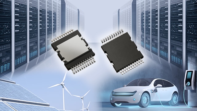
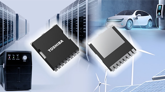
3rd generation Silicon Carbide(SiC) MOSFETs
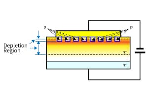
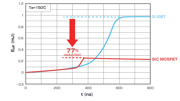
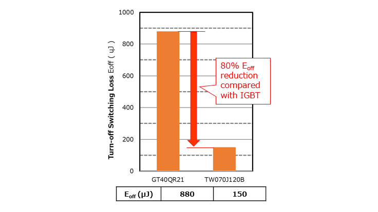
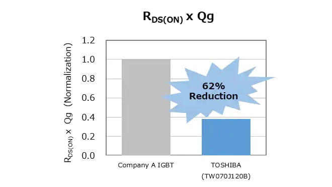
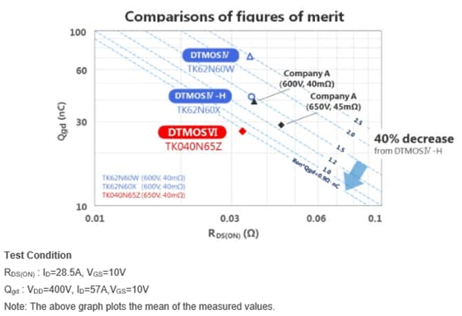
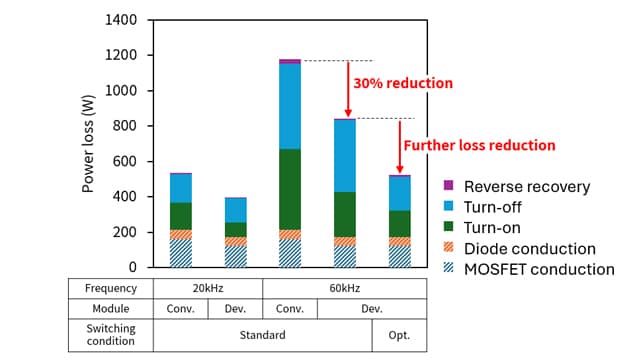
Toshiba's 3rd generation Silicon Carbide (SiC) MOSFETs introduces a selection of both 650V and 1200V voltage products. In common with 2nd generations, Toshiba's newest generation of MOSFETs include a built-in SiC Schottky Barrier Diode (SBD) with a low forward voltage (VF) of -1.35V (typ.), placed in parallel with the PN diode in the SiC MOSFETs, to suppress fluctuation in RDS(on) thereby enhancing reliability. Furthermore, Toshiba’s advanced SiC process[1] has greatly improved our on-resistance per unit area RonA, and the performance index Ron*Qgd, which indicates switching characteristics, compared to 2nd generation products. Also, it has easy to design gate drive circuit, and you can prevent malfunctions due to switching noise.
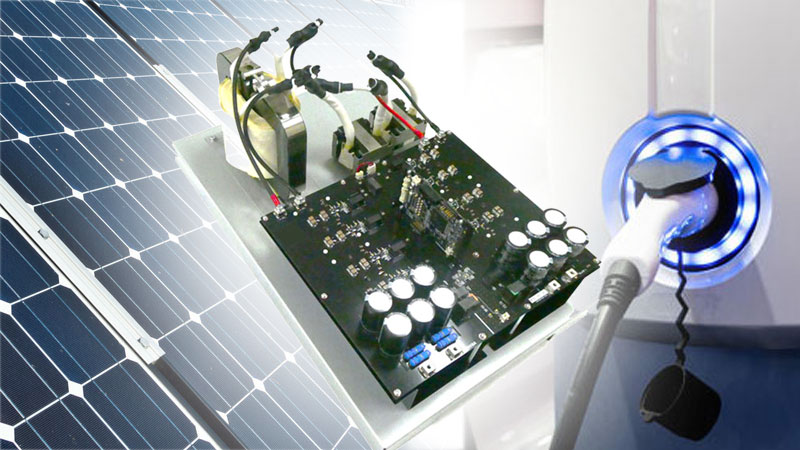
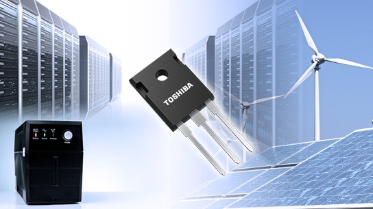
Toshiba's 3rd generation SiC MOSFETs provides lower power consumption and supports higher power density for applications such as switching power supplies (servers for data centers, communication equipment, etc.), uninterruptible power supplies (UPS), PV inverters, EV charging stations, etc.
Toshiba's 3rd generation SiC MOSFETs provides lower power consumption and supports higher power density for applications such as switching power supplies (servers for data centers, communication equipment, etc.), uninterruptible power supplies (UPS), PV inverters, EV charging stations, etc.
-mosfets_features_1_en.png)
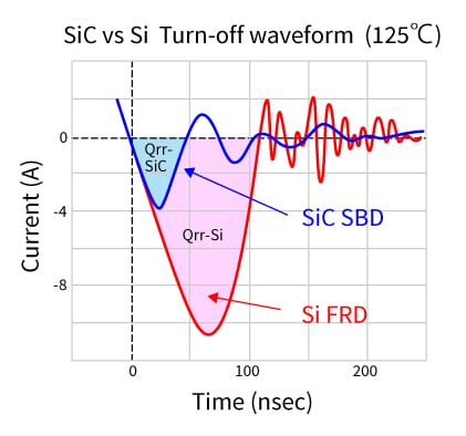
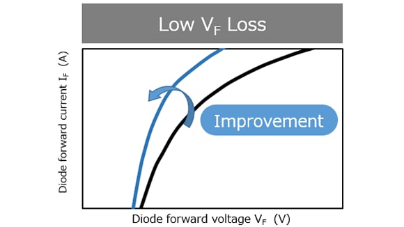
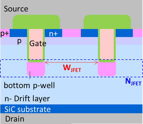
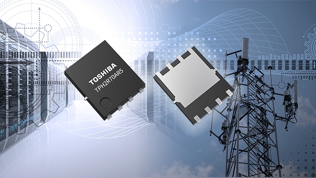
3rd generation SiC Schottky barrier diode (SBD)
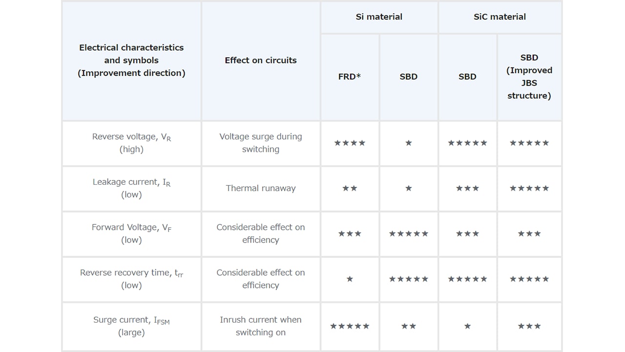
It adopts the new schottky metal, and it is equipped with 3rd generation SiC SBD chip, which optimized junction barrier schottky (JBS) structure of 2nd generation. As a result, we have achieved industry-leading lowest forward voltage 1.2V (Typ.) for 650V products, and 1.27V (Typ.) for 1200V products. For the 650V products, the 3rd generation products have improved the trade-offs between forward voltage and total capacitive charge, and the trade-offs between forward voltage and reverse current compared with the 2nd generation products. This reduces power dissipation and contributes to high efficiency of equipment.
SBD*:Schottky Barrier Diodes


種類
應用手冊
Technical topics
參考設計


模擬
Related information
開啟新視窗